


For the Heat Pass Block to work, DRAM had to be moved from the top of the die
The HPB is a copper heat sink that is placed on top of the processor, forcing DRAM to find a new location. The latter was moved to the side of the AP so that the HPB and the processor could make direct contact. Additionally, having DRAM sit on top of the chipset, while saving space, makes the AP too hot. Thanks to thermal conduction, the heat generated by the Exynos 2600 is transferred to the base of the heat sink, making the SoC 30% cooler.
The HPB allowed the Exynos 2600 to outperform a Snapdragon 8 Elite Gen 5 cooled by liquid nitrogen
This test used a pair of Galaxy S26+ units because the Galaxy S26 Ultra is powered by Qualcomm’s chip in all markets. This is important because the Galaxy S26+ doesn’t use the same vapor chamber as the larger Galaxy S26 Ultra model, and the Exynos 2600 did suffer from thermal throttling.
Rival chip designers have been taking note of the HPB
The new design for the Exynos 2700 returns RAM to the top of the SoC with the heat sink placed on top of RAM. This will not only cool down the CPU but also RAM.
The Exynos 2600 powering the Galaxy S26 and Galaxy S26+ was the first 2nm silicon to be used to drive a smartphone. That broke Apple’s recent string of being the first to debut the next level of cutting-edge processors, as the iPhone XS and XS Max were the first with a 7nm AP (A12 Bionic) in 2018 (as a footnote, the Huawei Mate 20 series was the first to announce a 7nm processor with the Kirin 980 but it was beaten to the marketplace by Apple).
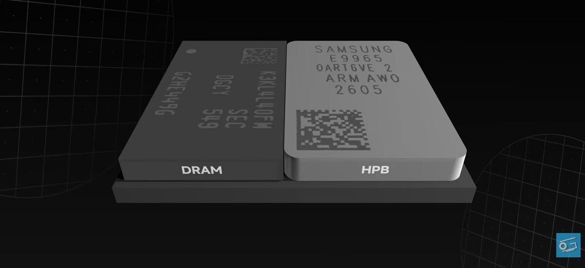
Illustration shows the placement of the Heat Pass Block next to RAM on the Exynos 2600. | Image by Geekerwan
The Exynos 2600 used Samsung Foundry’s SF2 2nm process node, which also debuted the Gate-All-Around (GAA) transistor architecture. The Gate covers the channel on all four sides reducing current leak and improving the drive current. The higher the drive current, the faster the transistor can change its state from “On” to “Off”, improving the performance of the chip.
Exynos 2700 will be produced using Samsung Foundry’s enhanced 2nm process node
The Exynos 2700 will use Samsung Foundry’s enhanced SF2P process node, expected to result in a 12% improvement in gross performance and a 25% reduction in energy consumption compared to the SF2 process.
So it would appear as though Samsung has been slowly improving its Exynos AP to the point that the major flaw it had, overheating resulting in CPU throttling, is less of a problem than before. The HPB was a brilliant idea, and we could see it added to chip designs from companies like Apple and Qualcomm.
